Gold tin solder and its application in the field of electronic device packaging
Gold tin solder and its application in the field of electronic device packaging
Brazing is an important technology for assembling electronic products. In order to obtain the ideal brazing connection, the choice of brazing material is very important. Solderability, melting point, strength, Young's modulus, coefficient of thermal expansion, thermal fatigue, creep and creep resistance of brazing materials can affect the quality of brazing joints.
Apex-New Material's gold 80% Tin 20% brazing alloy (melting point 280 ° C) has been used for many years in the semiconductor and other industries. Due to its excellent physical properties, gold-tin alloy has gradually become the best brazing material for the packaging of optoelectronic devices.
2 Au80%Sn20% physical core energy of solder
Some basic physical properties of AU80%SN20%Gold tin solder.
(1) brazing temperature is moderate
The brazing temperature is only 20 ~ 30℃ higher than its melting point (that is, about 300 ~ 310). In the process of brazing, due to the eutectic composition of the alloy, a small superheat can melt and infiltrate the alloy; In addition, the solidification process of the alloy is also very fast. Therefore, the use of gold tin alloy can greatly shorten the entire brazing process cycle. The soldering temperature range of gold tin alloys is suitable for the assembly of components with high stability requirements. At the same time, these components can also withstand subsequent assembly using lead-free solder at relatively lower temperatures. The solder is assembled at a temperature of approximately 260 ° C.
(2) High strength
At room temperature, the yield strength of gold-tin alloys is very high. Even at a temperature of 250 ~ 260 ° C, its strength can meet the requirements of air tightness. The strength of the material is comparable to that of some high-temperature brazing materials, but the brazing process can be done at relatively much lower temperatures.
(3) No flux is required
Due to the large proportion of gold in the alloy composition (80%), the oxidation degree of the material surface is low. If a vacuum is used in the brazing process, or a mixture of reducing gases such as nitrogen and hydrogen, chemical flux is not necessary.
(4) It has good wettability and corrosion of lead-free solder with gold plating
The composition of gold-tin alloys is similar to that of gold plating, but the degree of leaching of very thin coatings through diffusion is very low, and there is no migration phenomenon like silver.
(5) Low viscosity
Liquid gold tin alloys have very low viscosity and can fill some large voids.
In addition, Au80% Sn20% solder also has high corrosion resistance, high creep resistance and good thermal and electrical conductivity. The disadvantage of Au80%Sn20% solder is that its price is more expensive, its performance is more brittle, its elongation is very small, and it is not easy to process.
")
3 Thermodynamic properties
Since the thermodynamic properties of gold-tin alloy determine many of its useful properties, it is necessary to understand some basic thermodynamic properties of the alloy. Gold tin can form a eutectic alloy with a composition ratio of 80 wt % gold to 20 wt % tin.
Jinxi alloy at 280 ℃ of eutectic reaction in liquid phase L < - > zeta + delta. Near the reaction in alloy, mainly includes the zeta '(Au5Sn), zeta and delta (AuSn) phase. In the ζ "" phase, the weight percentage of tin is 10.7%. It has a hexagonal structure and is a stable phase below 190 ° C. The ζ phase is formed by the peritectic reaction β+L<-->ζ. At 521℃, the weight percentage of tin in ζ phase is 5.7%. At 280℃, the percentage is 11.3%; At 190℃, the 8.8% zeta phase has a magnesium-type hexagonal close-packed structure. Phase ζ is a metallic compound with a melting point of 419.3℃ and a NiAS-type hexagonal structure. The composition of the δ phase can fluctuate within a range of 50.0% to 50.5% atomic percentage of tin (37.5% to 37.9% by weight).
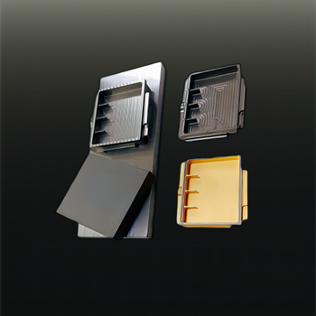
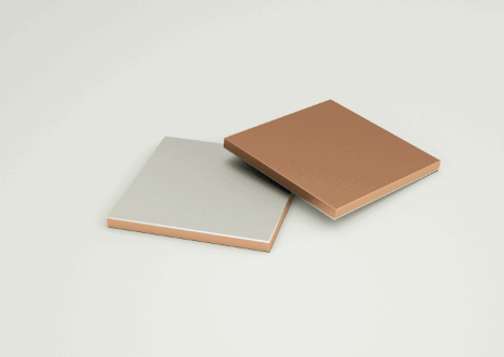
4 Gold tin solder preformed sheet
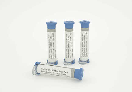
There are many forms of brazing materials that can be used for microelectronic packaging, the most important forms are wire, sheet, solder paste and preformed sheet. Due to the very brittle nature of gold-tin alloys, these forms of wire or sheet are difficult to process according to specifications. In the process of processing often also cause waste of materials, require a lot of labor, while the quality situation is also very inconsistent. Of all these forms, brazing paste is the most ideal form for electronic packaging. However, one of the components of brazing paste is flux, which is prohibited in many application areas. Even when flux can be used, the residue of the assembled components is cleaned after the brazing process is complete. Therefore, in order to obtain stability for applications such as device production and packaging, the right choice should be stamped preformed sheets. The preformed sheet ensures the exact amount and location of the solder to achieve the best quality at the lowest cost. In the 1960s, preformed sheets were first used to produce components such as metal-encapsulated tantalum capacitors. At present, it is mainly used in the production and packaging process of passive components and optoelectronic devices. The preformed sheet has the following advantages:
By using the preforming method, it can precisely control the amount of brazing material, composition and surface state, thereby providing a larger brazing process window and the best assembly quality to obtain the improvement of brazing connection reliability, which is the high Cpk value and low cost under guaranteed quality conditions usually required by the industry.
② The use of preformed sheets in a controlled atmosphere can eliminate the use of easily contaminated and difficult to control flux. By controlling the soldering process, the costly cleaning process after welding can be eliminated at the same time.
Preformed sheets are usually the best solution for high-performance welding that requires high reliability and good thermal conductivity.
④ For the changes in the substrate material that need to be connected and the requirements of special performance or environmental protection, there are almost no restrictions on the Jinxi solder preformed sheet.
⑤ After correct design and application, the preformed sheet can obtain a higher performance-to-price ratio, so that the welding point has a high yield and electrical reliability.
5 Application of AuSn pads
Because the melting point of the eutectic solder (280 ° C) is much higher than that of the SN96.5%AG3.5%SN-AG eutectic solder (221 ° C), it cannot be used at the same temperature as the organic materials widely used in electronic packaging. However, the gold solder is best for some special applications that require both mechanical and thermal conductivity to achieve high reliability Select. These applications include airtight caps, optoelectronics | RF and DC isolation bonding in laser device packaging processes, laser diode core bonding, etc.
Part of the airtight electronic package product needs to be welded to some ceramic parts. In this case, the main consideration is that ceramics have some physical properties that metal parts cannot achieve, such as low thermal expansion coefficient, electrical insulation, high strength and so on. One application is to glue the active device chip into a housing when both the active device chip and the substrate need to have a low coefficient of thermal expansion. In this case, a stamped gold tin prefabricated sheet about 25μm thick can be used as the solder. Another application in ceramic packaging is the cover, which is to seal a metal or glass cover plate to a ceramic housing. At this time, a 25μm thick gold tin preformed sheet with an unclosed frame is also selected. For the cover, a parallel seam welder is generally used to locally heat the joint. This will not affect the active device chip brazed with gold tin alloy in the package. A third ceramic application is the welding of lead insulators. At this time, high-strength ceramic, rather than glass, is used as an insulator. For these applications, the brazing material is required to have good wettability, corrosion resistance and high Young's modulus. The high Young's modulus ensures that the material can be processed very thin but still remain flat over a large area. As previously mentioned, the surface of the gold tin preform sheet is clean and oxide free, allowing for a production process without flux. Even if the substrate surface is slightly oxidized, a mixture of nitrogen and hydrogen gases can be used to remove oxides. After the oxide is removed, the pre-formed sheet can be heated and melted to begin the welding process. Usually above 235 ° C, it is very effective to remove oxides with a mixture of nitrogen and hydrogen. However, if a low melting point brazing material is used (for example, below 235 ° C, at which temperature the nitrogen hydrogen mixture does not work), the oxide on the substrate surface will be present at the weld. This is one of the main reasons for some poor welding quality. Devices welded with gold-tin alloys can withstand prolonged thermal stress cycles.
In the through-bonding of photoelectric devices such as transmitter, receiver and amplifier package, gasket type gold tin preform is the best choice. During the connection process, the melted gold tin washer, under capillary action, fills the gap between the outer conductor of the insulator and the package substrate (both made of Corvar alloy and plated with nickel and gold). Because the gap between the insulator and the substrate is very small, too much brazing material will cause a short circuit. As one of the advantages of preformed sheets, a precise amount of gold and tin solder can be made into gasket preformed sheets to prevent short circuits.
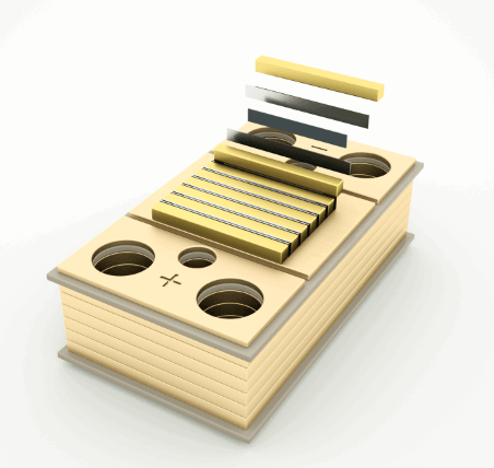
In the assembly of high power laser diode (LD) with tube core bonding technology, the use of gold tin preform has been accepted by more and more manufacturers. As shown in Figure 4, the laser diode chip and copper heat sink are welded by a gold tin preform sheet. Since the luminous efficiency of the laser diode decreases sharply with the increase of temperature, it is very important to dissipate the heat generated by the diode when it emits light in time, and the excellent thermal conductivity of the gold tin solder can play a very effective role here to ensure the best performance of the laser diode. In addition, because of the high Young's modulus of gold tin alloy, even in the case of very thin (5 ~ 25μm), it can maintain flatness and a certain bending resistance. Therefore, the possibility of fire and impurity pores in the welding layer is greatly reduced during the welding process, and the thermal resistance of the welding point is reduced, which greatly improves the reliability of the laser diode. In flip chip welding, due to the connection between the source area of the device and the substrate, the excellent thermal and electrical conductivity of the gold-tin alloy is particularly important. In addition, gold-tin alloy preformed sheets are also used in microwave system assembly and other fields. As the excellent properties of gold tin alloy and the advantages of its preformed sheet are more and more recognized, its application in the field of packaging will become more extensive and important.
6 Precautions in the use of gold 80% tin 20% solder
Gold tin solder must be used correctly in order to obtain good results. The main factors affecting welding quality are: gold solder composition, solder and solder surface quality (such as oxide, stain, flatness, etc.), process factors (furnace temperature wire, maximum temperature, gas composition, working fixture, etc.)[2]. It can be seen from Figure 1 that the melting point of gold-tin alloy is very sensitive to the composition near the eutectic temperature. When the weight ratio of gold is greater than 80%, the melting point increases sharply with the increase of gold. The welded parts often have a gold-plated layer, and the gold of the gold-plated layer will be immersed in the solder during the welding process. In the case of too thick gold-plated layer, too thin preformed solder, and too long welding time, the gold leaching into the solder will increase, and the melting point will rise. Therefore, all the above welding parameters need to be optimized [2]. Generally, the peak temperature of the furnace should be selected at about 350 ° C. The welding time is 2 to 4 minutes. The welding yield can be above 98%.
Due to the moderate melting point (280℃) of gold 80% tin 20% eutectic alloy, high strength, no flux, good thermal and electrical conductivity, excellent wettability, low viscosity, easy welding, corrosion resistance, creep resistance, etc., it is used in ceramic packaging and sealing of microelectronic devices and optoelectronic devices, chip bonding, metal packaging ceramic insulator welding, high-power semiconductor laser chip welding The connection has a wide range of applications, which can significantly improve the package reliability and electrical/thermal conductivity of these devices.